Showing posts with label Analog and Digital Electronics. Show all posts

Thursday, October 13, 2011

C167 Microcontroller Basics- Components and Design process

1. The Brains

I already explain the brains of the robot to be a controller, in other words, a microprocessor. Hold on! Don’t start thinking Gigahertz processors! A 20 MHz processor would suffice! In your case, it is the Infineon C167CR-LM (henceforth referred to as the C167). 

2. What is the C167?
Glad you asked! Figure 1 shows the location of the microcontroller on the KitCON-167 board from Phytec (more on this board later). You can open your CalBOT kit and examine this board as you read this article. Don’t worry if your board is not all wired up like mine.


Figure 1. The actual C167CR-LM on my board.

The C167 is a microcontroller, it is used to control (makes sense!) some process or aspect of the environment. Just like the more popular microprocessor (the Intel Pentium or the AMD Athlon), a microcontroller has a lot of stuff built into it – o n-chip memory, an Arithmetic Logic Unit (ALU) etc. However, unlike the Pentium a microcontroller is not optimized for building PCs or laptops. For instance, the maximum clock speed of your C167 is 20 MHz. The latest Pentiums on the other hand have clock speeds in the Gigahertz range. But this speed is required only for computationally intensive software. The software controlling your CalBOT is not that complex. 20 MHz is a very fast clock speed for a microcontroller.

Clock speed is not the only area where microcontrollers differ from microprocessors. The C167 has other components suited for control that are built onchip, which the Pentium does not have. Examples include Analog-to-Digital converter (A/D module), the ASC0 (Asynchronous serial transmitter) and the PWM (Pulse Width Modulation unit). Of these modules, only the PWM is covered in detail in this manual.The reason is twofold: you only need to understand the PWM module to complete the basic CalBOT and more importantly, to avoid repetition. Once you understand one module, it is a simple matter to look up how the other modules work and then use them. 

Just like you need a motherboard to build a computer, the C167 needs a target board so its potential can be fully realized. We use the KitCON-167, this is the board on which the C167 is mounted. Figure 2 shows the different parts of the KitCON-167.
Figure 2. The most important components of the KitCON-167. The rectangles associate the description with the components.

Of the components shown in figure 2, you need to be familiar only with the KitCON connector to complete the CalBOT. You don’t need to understand the details of voltage regulation, RS-232 protocols or the memory architecture!

3.  Using the C167
Using the C167 (or any microcontroller) is mainly a four-step process.  First, you program the module you want (for instance, the PWM).  Then you download this code to the on-board RAM.  You test your code.  If there is an error, you start the debugging process.  Once you are satisfied your C167 is doing what yo u want, you have the option of burning your code to FLASH so your code is retained even when you turn off the power.  Figure 3 summarizes the build process.  We will expand upon these steps in greater detail as we move along in the manual.  However, burning code to onboard FLASH is not covered in this manual.
Figure 3.  The design process

Tuesday, October 4, 2011

How to use the Breadboard to make Electronic circuits?


Uses of Breadboard
A breadboard is used to make up temporary circuits for testing or to try out an idea. No soldering is required so it is easy to change connections and replace components. Parts will not be damaged so they will be available to re-use afterwards.Almost all the Electronics Club projects started life on a breadboard to check that the circuit worked as intended.

Connections on Breadboard
The photograph shows a typical small breadboard which is suitable for beginners building simple circuits with one or two ICs (chips). Larger sizes are available and you may wish to buy one of these to start with.

Breadboards have many tiny sockets (called 'holes') arranged on a 0.1" grid. The leads of most components can be pushed straight into the holes. ICs are inserted across the central gap with their notch or dot to the left.

Wire links can be made with single-core plastic-coated wire of 0.6mm diameter (the standard size). Stranded wire is not suitable because it will crumple when pushed into a hole and it may damage the board if strands break off. The diagram shows how the breadboard holes are connected:

The top and bottom rows are linked horizontally all the way across as shown by the red andblack lines on the diagram. The power supply is connected to these rows, + at the top and 0V (zero volts) at the bottom.

I suggest using the upper row of the bottom pair for 0V, then you can use the lower row for the negative supply with circuits requiring a dual supply (e.g. +9V, 0V, -9V).

The other holes are linked vertically in blocks of 5 with no link across the centre as shown by the blue lines on the diagram. Notice how there are separate blocks of connections to each pin of ICs.

Large Breaboards
On larger breadboards there may be a break halfway along the top and bottom power supply rows. It is a good idea to link across the gap before you start to build a circuit, otherwise you may forget and part of your circuit will have no power! 


Building a Circuit on Breadboard
Converting a circuit diagram to a breadboard layout is not straightforward because the arrangement of components on breadboard will look quite different from the circuit diagram.

When putting parts on breadboard you must concentrate on their connections, not their positions on the circuit diagram. The IC (chip) is a good starting point so place it in the centre of the breadboard and work round it pin by pin, putting in all the connections and components for each pin in turn.

Monostable Circuit Diagram 

The best way to explain this is by example, so the process of building this 555 timer circuit on breadboard is listed step-by-step below.

The circuit is a monostable which means it will turn on the LED for about 5 seconds when the 'trigger' button is pressed. The time period is determined by R1 and C1 and you may wish to try changing their values. R1 should be in the range 1k to 1M.

Time Period, T = 1.1 × R1 × C1

IC pin numbers
IC pins are numbered anti-clockwise around the IC starting near the notch or dot. The diagram shows the numbering for 8-pin and 14-pin ICs, but the principle is the same for all sizes.

Components without suitable leadsSome components such as switches and variable resistors do not have suitable leads of their own so you must solder some on yourself. Use single-core plastic-coated wire of 0.6mm diameter (the standard size). Stranded wire is not suitable because it will crumple when pushed into a hole and it may damage the board if strands break off.

Building the example circuit Begin by carefully insert the 555 IC in the centre of the breadboard with its notch or dot to the left.Then deal with each pin of the 555:

Monostable Circuit on Breadboard 

  • Connect a wire (black) to 0V. 
  • Connect the 10k resistor to +9V. 
  • Connect a push switch to 0V (you will need to solder leads onto the switch) 
  • Connect the 470 resistor to an used block of 5 holes, then... 
  • Connect an LED (any colour) from that block to 0V (short lead to 0V). 
  • Connect a wire (red) to +9V. 
  • Connect the 0.01µF capacitor to 0V. 
  • You will probably find that its leads are too short to connect directly, so put in a wire link to an unused block of holes and connect to that. 
  • Connect the 100µF capacitor to 0V (+ lead to pin 6). 
  • Connect a wire (blue) to pin 7. 
  • Connect 47k resistor to +9V. 
  • Check: there should be a wire already connected to pin 6. 
  • Connect a wire (red) to +9V. Finally...
  • Check all the connections carefully. 
  • Check that parts are the correct way round (LED and 100µF capacitor). 
  • Check that no leads are touching (unless they connect to the same block). 
  • Connect the breadboard to a 9V supply and press the push switch to test the circuit.
 If your circuit does not work disconnect (or switch off) the power supply and very carefully re-check every connection against the circuit diagram.

Integrated Circuit Coding / Numbering


Introduction to Integrated Circuits(IC’s)

An integrated circuit can be defined generally as an arrangement of multifunction semiconductor devices. It consists of a single-crystal chip of silicon, nearly 1.5 mm2 in cross-section, containing both active and passive elements and their interconnections.
Earlier electronic circuits were assembled from individual components (e.g. resistor, capacitor, diode, transistors etc.) joined by wires. The sizes were further reduced by the use of printed circuit boards. The interconnection between various components is made through their metal strips formed on an insulating sheet. Such circuits are known as discrete circuits because each component of the circuit is separate from others. Main disadvantages of discrete circuits are that
  • they occupy large space
  • large number of soldered joints are less reliable
In an integrated circuit, various components such as resistors, capacitors, diodes etc. are fabricated on the same semiconductor chip. The reliability of the circuit is increased as the active and passive components are built in the same crystal. The most noticeable characteristic of an IC is its size. It is thousands of times smaller than a semiconductor structure built in the usual manner with discrete components
Our world is full of integrated circuits. You find several of them in computers. For example, the microprocessor is an integrated circuit that processes all information in the computer. It keeps track of what keys are pressed and if the mouse has been moved. It counts numbers and runs programs, games and the operating system. Integrated circuits are also found in almost every modern electrical device such as cars, television sets, CD players, cellular phones, etc.

Classification of Integrated Circuits
Integrated circuits can be divided into two general classes, linear (analogue) and digital. Typical examples of linear integrated circuits are operational amplifiers whereas typical examples of digital integrated circuits are the logic gates and microprocessors that you met in the earlier chapters. It’s worth noting that a number of integrated circuit devices bridge the gap between the analogue and digital world. Such devices include analogue to digital converters (ADC), digital to analogue converters (DAC), and timers.
Digital integrated circuits can contain anything from one to millions of logic gates, flip-flops, multiplexers, and other circuits in a few square millimeters. The small size of these circuits allows high speed, low power dissipation, and reduced manufacturing cost compared with board-level integration. These digital ICs, typically microprocessors, DSPs, and micro controllers, work using binary mathematics to process "one" and "zero" signals.
Analog ICs, such as sensors, power management circuits, and operational amplifiers, work by processing continuous signals. They perform functions like amplification, active filtering, demodulation, and mixing. Analog ICs ease the burden on circuit designers by having expertly designed analog circuits available instead of designing a difficult analog circuit from scratch.
Pin Numbering for various IC packages
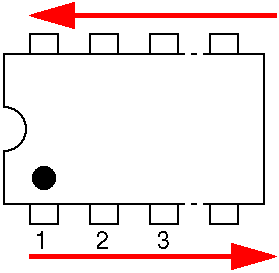
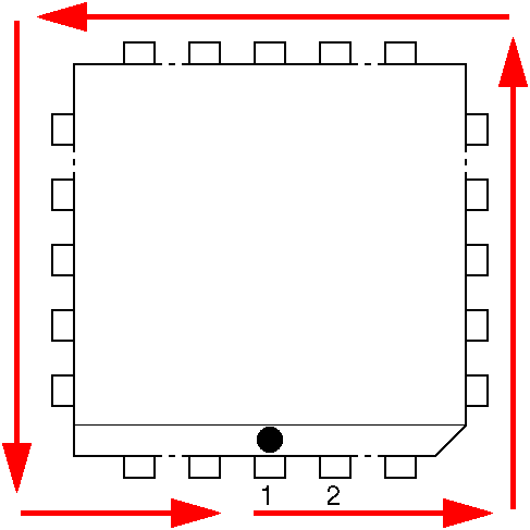
The pins are numbered anti-clockwise around the IC (chip) starting near the notch or dot. Often, but not always, GROUND and VCC are at opposite corners GROUND is usually on the lower left. VCC is usually on the upper right.
Examples of through-hole and surface-mounted devices. The DIP is larger than the SOIC with he same number of leads. 

Briefly looks some IC packages and their pin numbering,

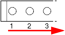
SIP package

SIP pin numbering
This numbering method is used for these packages:
  • SIP (Single In-line Package)
  • SIL (Single In-Line)


DIP package

DIP pin numbering
This numbering method is used for these packages:
  • DIP (Dual In-line Package)
  • DIL (Dual In-Line)
  • SDIP (Shrink Dual In-line Package)
  • SO (Small Outline)
  • SOIC (Small Outline Integrated Circuit)
  • SOJ (Small Outline J-leaded)
  • SOP (Small Outline Package)
  • SSOP (Shrink Small Outline Package)
  • TSOP (Thin Small Outline Package)


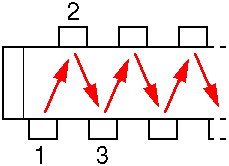
ZIP package

ZIP pin numbering 

  This numbering method is used for these packages:

  • ZIP (Zig-zag In-line Package)


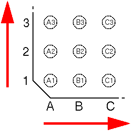
PGA package

PGA pin numbering
This numbering method is used for these packages:
  • PGA (Pin Grid Array)
  • BGA (Ball Grid Array)


PLCC package

PLCC pin numbering
This numbering method is used for these packages:


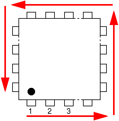
QFP package

QFP pin numbering
This numbering method is used for these packages:
  • QFP (Quad Flat Package)
  • PQFP (Plasic Quad Flat Package)
  • PLCC (Plasic Leaded Chip Carrier)