Showing posts with label Computer Architecture. Show all posts

Wednesday, October 19, 2011

How to Fix Boot Disk Failure? - Easy method

CauseThis issue could be caused by any of the below possibilities.
  1. Boot options are not set properly in CMOS
  2. Non bootable disc or USB in computer
  3. Remove added hardware /check connections
  4. Hard disk drive is bad

Solution

Boot options are not set properly in CMOS
Verify that the boot options within CMOS Setup are set properly. Below is an example of how we recommend the boot options be set.
  1. Floppy drive
  2. CD-ROM drive
  3. Hard Drive
  4. Other / Network
Non-bootable floppy diskette or disc or USB in computer
Verify that there is no floppy diskette or disc in the computer. If the boot options are set improperly the computer could be trying to boot from the disc drive instead of the hard drive.
In addition to verifying there is no disc in the computer make sure that no USB jump drive, external hard disk drive, or memory stick is inside any memory card reader.
If you're wanting to boot from a floppy diskette, CD, DVD, or USB drive and are getting this error message and have verified that your CMOS settings are in the proper order as explained in the above paragraph the diskette or disc you're using is either bad or does not have the proper files on it to make it bootable.

Remove added hardware / check connections
If you've recently installed any new hardware it's suggested that it be removed to verify it's not causing this issue. If after the device has been removed the computer works and it was another IDE / EIDE device ensure that the jumpers are properly set on the hard disk drive.
In addition to removing any new hardware it's also suggested if you've recently moved the computer or installed anything inside the computer that the connections for the drive be checked. Usually it's best to disconnect the cables from the back of the drive and reconnect them to make sure they're connected properly. While inside also disconnect and reconnect the cable connected to the motherboard as well. While inside your computer make sure you're aware of ESD.
Bad hard disk drive
If you have followed the above steps and you continue to experience the same issue, unfortunately it is likely that the hard disk drive is bad or the controller is bad.
If available, you may want to connect another known good hard disk drive to the computer to determine if it can be detected. If it is able to be detected then replace your hard disk drive. If it is not detected, unfortunately you will need to replace the motherboard or controller as it is bad.
If no additional hard disk drive is available it is recommended that the hard disk drive be replaced first or that the computer be serviced / repaired.

Monday, October 10, 2011

The Architectural trends in today’s Microprocessor.

Introduction to Today’s Microprocessor trends

From their humble beginning 25 years ago, microprocessors have proliferated into an astounding range of chips, powering devices ranging from telephones to supercomputers. Today, microprocessors for personal computers get widespread attention--and have enabled Intel to become the world's largest semiconductor maker. In addition, embedded microprocessors are at the heart of a diverse range of devices that have become staples of affluent consumers worldwide.
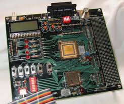
The past decade has seen the evolution of microprocessor packaging from a simple protective scheme to a complex combination of different elements that enable microprocessor performance while still providing the basic function of protection. Packaging today's microprocessor on the one hand entails tailoring the package to enable microprocessor performance, a complex task considering the rapid rate of microprocessor performance growth. This challenge is in terms of schedule and technical complexity. On the other hand, the package forms the interface between the microprocessor and the external world of the motherboard and the computing system. In this capacity, package design must allow for an easy interface and must meet a diverse set of form factor requirements.

The package provides a conduit for the microprocessor through a space transformation allowing small-scale features on the silicon to be electrically connected to the external environment. This is a challenging geometrical problem and requires that packaging interconnection densities must closely track the evolution of microprocessor interconnection densities. In connecting the die to the motherboard, the package must also ensure that the connections do not unduly inhibit the microprocessor performance by introducing unnecessary electrical impediments usually referred to as package “parasitics.” As microprocessors have evolved, they have increased in speed, which in turn needs increasingly sophisticated power delivery schemes. Another consequence of microprocessor evolution has been increasing power dissipation. Package design must now provide a path for thermal dissipation, requiring a better understanding of the thermal characteristics of packaging materials and design. Package design also requires a good understanding of the structural characteristics of the package to ensure it is designed for reliability and robustness. Attention is increasingly focussed today on understanding the electrical, thermal and mechanical characteristics of packaging to optimize all these aspects.

The package is also the interface that connects the microprocessor to the motherboard. In this capacity it must have a compatible interface to allow for easy acceptance on the motherboard as well as the system design. The form factor of the package is a critical element for easy interface to the motherboard. The requirements are usually different in different market segments and often drive the need for form factors that are tailored to these different segments. For instance, the height of the package is critical to enable a microprocessor in a mobile market where a slim and low weight package is critical to success. On the other hand, the ability to dissipate high power, and hence features that enables this, are critical in a server or desktop market segment. Cost, compatibility and fit within the computer system are key parameters that must be designed for in making a microprocessor successful. This challenges us into concurrently developing multiple solutions and technologies geared towards specific market segments.

Aside from the challenges of package design, there is a need to develop efficient and cost-effective manufacturing processes that allow us to meet the schedule and volume demands of today's market places. These have presented us with interesting challenges in understanding the manufacturability, testability and reliability of packaging. Some of these issues are discussed in greater detail in this issue.

MAJC is an example of the design architecture of today’s microprocessor. We can easily related to the current trend by analysing the architecture of MAJC .

MAJC (pronounced "magic") is an acronym for "Microprocessor Architecture for Java Computing." MAJC is a microprocessor architecture designed to meet the broadband demands of the 21st century. Addressing the challenge of high bandwidth and the need for state-of-the-art computational performance, MAJC architecture is characterized by:
  • Scalability to take full advantage of advances in semiconductor technology.
  • Broad scalabilty to systems with large numbers of processors.
  • A new standard of performance for applications with DSP or New Media computational needs.
  • Focus on bandwidth throughput.

Processor Needs into the 21st Century
Several microprocessor trends were identified and accommodated in the design of the MAJC Architecture:
  • Convergence of communication media and computers (audio, video, and data) require processors to compute information at wire speed.
  • Advancements in semiconductor technology will provide rapidly-increasing resources on each microprocessor chip.
  • As microprocessors are used in increasingly disparate applications from smart cards to supercomputers there is great value in the ability to create a wide span of implementations from a given processor architecture.
  • Software, over time, will become independent of specific instruction sets; Just-In-Time (JIT) compilation techniques are expected to predominate for general-purpose processors and eliminate binary compatibility issues.
  • Bandwidth between processors, memory, and I/O devices needs to be available to move information in real-time.
  • The content processed by computers is becoming increasingly media-rich; DSP-like functions are required to process this media content.

Features of Today’s Microprocessors.
  • Modular Architecture
To support the creation of a wide range of implementations the architecture supports modular implementations. A basic implementation might comprise a single processor unit with four functional units. By replicating those design elements, an implementation can be built that includes a few or even hundreds of processors, each with four functional units, each of which can operate on many data items simultaneously with parallel-operation (SIMD) instructions. Conversely, a tiny application-specific implementation can be derived from the basic one by trimming the complement of functional units down to one or two and/or removing hardware support for any instructions not needed in its target application.
  • Software Portability
The architecture was designed to efficiently execute code generated by installation-time or just-in-time (JIT) compilation techniques. It may be the first commercial architecture designed without a requirement for binary compatibility between generations. This allows implementations to evolve over time without accumulating the baggage required to support old binaries, as traditional architectures have always done. Instead, software portability across implementations is obtained through use of architecture-neutral means of software distribution.
  • Multiple Levels of Parallelism
The architecture provides the ability to exploit parallelism at many levels - at the data word level through SIMD instructions, at the instruction level through multiple functional units per processor, at the thread-of-execution level through support for multithreaded software, and at the system level through its intrinsic support for "MPs-on-a-chip" (multiple processor units per implementation). A implementation with more than one functional unit per processor unit provides MSIMD: multiple single-instruction multiple-data parallelism.
  • Multiple Processor Units per Cluster
Although a MAJC implementation can be a single processor unit, the architecture explicitly incorporates the concept of multiple processors per implementation. Given 21st century semiconductor density, each such array of processor units or "processor cluster" can be implemented on a single chip. As semiconductor technology advances, clusters with more processors per chip can be implemented.
  • Multiple Functional Units per Processor Unit
Every MAJC processor unit can issue multiple instructions simultaneously, one to each of its functional units. Most implementations are expected to provide two to four functional units per processor unit.
  • Multithreaded Software
Execution of multithreaded software comes naturally given the architecture's ability to execute multiple threads simultaneously on multiple processor units. MAJC implementations with hardware support for vertical microthreading can efficiently execute multiple threads on each processor unit.
  • SIMD Instructions
At the lowest level of parallelism, MAJC architecture provides SIMD (Single Instruction/ Multiple Data) or "vector" instructions. A SIMD instruction executing in a single functional unit could perform the same operation on multiple data items simultaneously.
  • Integral Support for Media-Rich Data
The MAJC architecture is particularly well-suited for processing media-rich content because it directly supports common media data types and can process multiple simultaneous operations on that data. Processing power is multiplied on three levels: Single Instruction/Multiple Data (SIMD) DSP-like instructions in each functional unit, multiple functional units per processor unit, and multiple processor units per processor cluster.
  • Balanced Performance: Processor versus Memory and I/O
A MAJC implementation is designed to utilize several techniques to balance processor speed with access to external memory and I/O devices:
  • 100's of general-purpose registers per processor unit, which reduce the frequency of memory accesses
  • Load-Group instructions, which increase bandwidth into the processor by simultaneously loading multiple registers from memory or an I/O device
  • Store buffering, which increases bandwidth out of the processor by optimizing Store operations initiated by software
  • Data Type-Independent Registers
The general-purpose register file in a MAJC implementation is datatype-agnostic: any register can hold information of any data type and be accessed by any instruction. In particular, there is no distinction between integer and floating-point registers. This allows registers to be allocated as needed by each application, without restrictions imposed by hardware partitioning of the register set.
  • Instruction Grouping
Grouping instructions across multiple functional units can be performed dynamically in hardware (as in a superscalar processor), statically by a compiler, or by some combination of the two. Rather than devoting valuable chip area to hardware grouping logic, MAJC relies primarily on software compilers to group instructions across functional units.
  • Data and Address Size
A MAJC implementation may implement either 32- or 64-bit addressing and data operations, as dictated by the needs of its target applications.
  • Context Switch Optimization
Process (task) context switch time can be reduced by using the architecture's "register dirty bits", which allow an operating system to minimize the number of registers saved and restored during a context switch.

Memory Byte Order
The MAJC architecture's native byte order is "big-endian"; that is, multibyte values are stored in memory with the most significant byte at the lowest address and the least significant byte at the highest address. However, a MAJC implementation can manipulate data stored in any memory byte-order (notably "little-endian"). The BYTESHUFFLE instruction can reorder bytes efficiently in an arbitrary manner. Also, an implementation may define an Alternate Space Identifier (ASI) dedicated to performing automatic byte reordering whenever corresponding Load and Store from Alternate Address Space instructions are executed.

The architecture of Pentium Microprocessor

A Brief History of the Pentium Processor Family


The Pentium family of processors, which has its roots in the Intel486(TM) processor, uses the Intel486 instruction set (with a few additional instructions). The term ''Pentium processor'' refers to a family of microprocessors that share a common architecture and instruction set. The first Pentium processors (the P5 variety) were introduced in 1993. This 5.0-V processor was fabricated in 0.8-micron bipolar complementary metal oxide semiconductor (BiCMOS) technology. The P5 processor runs at a clock frequency of either 60 or 66 MHz and has 3.1 million transistors.

The next version of the Pentium processor family, the P54C processor, was introduced in 1994. The P54C processors are fabricated in 3.3-V, 0.6-micron BiCMOS technology. The P54C processor also has System Management Mode (SMM) for advanced power management

The Intel Pentium processor, like its predecessor the Intel486 microprocessor, is fully software compatible with the installed base of over 100 million compatible Intel architecture systems. In addition, the Intel Pentium processor provides new levels of performance to new and existing software through a reimplementation of the Intel 32-bit instruction set architecture using the latest, most advanced, design techniques. Optimized, dual execution units provide one-clock execution for "core" instructions, while advanced technology, such as super scalar architecture, branch prediction, and execution pipelining, enables multiple instructions to execute in parallel with high efficiency. Separate code and data caches combined with wide 128-bit and 256-bit internal data paths and a 64-bit, burstable, external bus allow these performance levels to be sustained in cost-effective systems. The application of this advanced technology in the Intel Pentium processor brings "state of the art" performance and capability to existing Intel architecture software as well as new and advanced applications.

The Pentium processor has two primary operating modes and a "system management mode."

The operating mode determines which instructions and architectural features are accessible.

These modes are:
  • Protected Mode
This is the native state of the microprocessor. In this mode all instructions and architectural features are available, providing the highest performance and capability. This is the recommended mode that all new applications and operating systems should target. Among the capabilities of protected mode is the ability to directly execute "real-address mode" 8086 software in a protected, multi-tasking environment. This feature is known as Virtual-8086 "mode" (or "V86 mode"). Virtual-8086 "mode" however, is not actually a processor "mode," it is in fact an attribute which can be enabled for any task (with appropriate software) while in protected mode.
  • Real-Address Mode (also called "real mode")
This mode provides the programming environment of the Intel 8086 processor, with a few extensions (such as the ability to break out of this mode). Reset initialization places the processor in real mode where, with a single instruction, it can switch to protected mode.
  • System Management Mode
The Pentium microprocessor also provides support for System Management Mode (SMM). SMM is a standard architectural feature unique to all new Intel microprocessors, beginning with the Intel386 SL processor, which provides an operating-system and application independent and transparent mechanism to implement system power management and OEM differentiation features. SMM is entered through activation of an external interrupt pin (SMI#), which switches the CPU to a separate address space while saving the entire context of the CPU. SMM-specific code may then be executed transparently. The operation is reversed upon returning.

Advanced Features
  • The Pentium P54C processor is the product of a marriage between the Pentium processor's architecture and Intel's 0.6-micron, 3.3-V BiCMOS process The Pentium processor achieves higher performance than the fastest Intel486 processor by making use of the following advanced technologies.
  • Superscalar Execution: The Intel486 processor can execute only one instruction at a time. With superscalar execution, the Pentium processor can sometimes execute two instructions simultaneously.
  • Pipeline Architecture: Like the Intel486 processor, the Pentium processor executes instructions in five stages. This staging, or pipelining, allows the processor to overlap multiple instructions so that it takes less time to execute two instructions in a row. Because of its superscalar architecture, the Pentium processor has two independent processor pipelines.
  • Branch Target Buffer: The Pentium processor fetches the branch target instruction before it executes the branch instruction.
  • Dual 8-KB On-Chip Caches: The Pentium processor has two separate 8-kilobyte (KB) caches on chip--one for instructions and one for data--which allows the Pentium processor to fetch data and instructions from the cache simultaneously.
  • Write-Back Cache: When data is modified; only the data in the cache is changed. Memory data is changed only when the Pentium processor replaces the modified data in the cache with a different set of data
  • 64-Bit Bus: With its 64-bit-wide external data bus (in contrast to the Intel486 processor's 32-bit- wide external bus) the Pentium processor can handle up to twice the data load of the Intel486 processor at the same clock frequency.
  • Instruction Optimization: The Pentium processor has been optimized to run critical instructions in fewer clock cycles than the Intel486 processor.
  • Floating-Point Optimization: The Pentium processor executes individual instructions faster through execution pipelining, which allows multiple floating-point instructions to be executed at the same time.
  • Pentium Extensions: The Pentium processor has fewer instruction set extensions than the Intel486 processors. The Pentium processor also has a set of extensions for multiprocessor (MP) operation. This makes a computer with multiple Pentium processors possible.
A Pentium system, with its wide, fast buses, advanced write-back cache/memory subsystem, and powerful processor, will deliver more power for today's software applications, and also optimize the performance of advanced 32-bit operating systems (such as Windows 95) and 32-bit software applications.

Friday, April 29, 2011

Computer Architecture


In computer science and computer engineering, computer architecture or digital computer organization is the conceptual design and fundamental operational structure of a computer system. It's a blueprint and functional description of requirements and design implementations for the various parts of a computer, focusing largely on the way by which the central processing unit (CPU) performs internally and accesses addresses in memory.
It may also be defined as the science and art of selecting and interconnecting hardware components to create computers that meet functional, performance and cost goals.
Computer architecture comprises at least three main subcategories:
  • Instruction set architecture, or ISA, is the abstract image of a computing system that is seen by a machine language (or assembly language) programmer, including the instruction set, word size, memory address modes, processor registers, and address and data formats.
  • Micro architecture, also known as Computer organization is a lower level, more concrete and detailed, description of the system that involves how the constituent parts of the system are interconnected and how they interoperate in order to implement the ISA. The size of a computer's cache for instance, is an organizational issue that generally has nothing to do with the ISA.
  • System Design which includes all of the other hardware components within a computing system such as:
  1. System interconnects such as computer buses and switches
  2. Memory controllers and hierarchies
  3. CPU off-load mechanisms such as direct memory access (DMA)
  4. Issues like multiprocessing.
Once both ISA and microarchitecture have been specified, the actual device needs to be designed into hardware. This design process is called the implementation. Implementation is usually not considered architectural definition, but rather hardware design engineering.
Implementation can be further broken down into three (not fully distinct) pieces:
  • Logic Implementation — design of blocks defined in the microarchitecture at (primarily) the register-transfer and gate levels.
  • Circuit Implementation — transistor-level design of basic elements (gates, multiplexers, latches etc.) as well as of some larger blocks (ALUs, caches etc.) that may be implemented at this level, or even (partly) at the physical level, for performance reasons.
  • Physical Implementation — physical circuits are drawn out, the different circuit components are placed in a chip floorplan or on a board and the wires connecting them are routed.
For CPUs, the entire implementation process is often called CPU design.
More specific usages of the term include more general wider-scale hardware architectures, such as cluster computing and Non-Uniform Memory Access (NUMA) architectures.